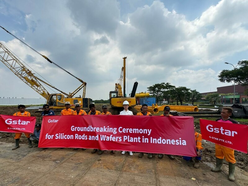
This move not only signifies a significant breakthrough for Gstar in its global photovoltaic industry layout but also represents remarkable progress in its industry chain vertical integration process.
Spanning 60,000 square meters, this modern factory is characterized by fully digitalized and intelligent production processes. The factory has introduced a series of cutting-edge production equipment and technologies, aiming at establishing a globally leading silicon wafer production base.
The factory will focus on monocrystalline silicon rods and large-sized silicon wafers of 182mm and 210mm, with broad prospects in the solar photovoltaic field. It will continuously drive technological innovation in the silicon wafer industry, particularly in large-sized, thin-film, and fine-line silicon wafers, providing higher quality and more efficient silicon wafers to global customers, thereby facilitating faster and more stable development of the photovoltaic industry.
The factory is expected to commence production by the end of 2024, achieving an annual production capacity of 3GW for crystal pulling and 3GW for slicing. This capacity will significantly support Gstar’s growth in the global photovoltaic component market, meeting the growing market demand and laying a solid foundation for the company’s long-term development.
Founded in 2019, Gstar is a technology company specializing in photovoltaic power generation solutions and a one-stop supplier of global mainstream photovoltaic products. It adheres to a strategy of industrial vertical integration, dedicated to independent research, development, design, production, and sales of silicon wafers, cells, frames, and modules. This vertically integrated model not only helps ensure product quality but also ensures supply chain stability, bringing price advantages and improving production efficiency. The groundbreaking construction of this silicon wafer factory is a significant step taken by Gstar under this strategic guidance.


